- 您现在的位置:买卖IC网 > Sheet目录357 > SI8631EC-B-IS1 (Silicon Laboratories Inc)IC ISOLATOR 3CH 3.75KV 16-SOIC
�� �
�
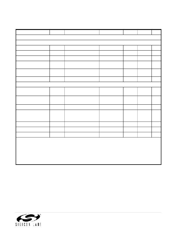
�Si8630/31/35�
�Table� 3.� Electrical� Characteristics� (Continued)�
�(V� DD1� =� 3.3� V� ±10%,� V� DD2� =� 3.3� V� ±10%,� T� A� =� –40� to� 125� °C)�
�Parameter�
�Symbol�
�Test� Condition�
�Min�
�Typ�
�Max�
�Unit�
�Timing� Characteristics�
�Si863xBx,� Ex�
�Maximum� Data� Rate�
�Minimum� Pulse� Width�
�0�
�—�
�—�
�—�
�150�
�5.0�
�Mbps�
�ns�
�Propagation� Delay�
�Pulse� Width� Distortion�
�|t� PLH� -� t� PHL� |�
�Propagation� Delay�
�Skew� 2�
�Channel-Channel� Skew�
�t� PHL� ,� t� PLH�
�PWD�
�t� PSK(P-P)�
�t� PSK�
�See� Figure� 2�
�See� Figure� 2�
�5.0�
�—�
�—�
�—�
�8.0�
�0.2�
�2.0�
�0.4�
�13�
�4.5�
�4.5�
�2.5�
�ns�
�ns�
�ns�
�ns�
�All� Models�
�Output� Rise� Time�
�Output� Fall� Time�
�Peak� Eye� Diagram� Jitter�
�Common� Mode�
�Transient� Immunity�
�Enable� to� Data� Valid�
�Enable� to� Data� Tri-State�
�t� r�
�t� f�
�t� JIT(PK)�
�CMTI�
�t� en1�
�t� en2�
�C� L� =� 15� pF�
�See� Figure� 2�
�C� L� =� 15� pF�
�See� Figure� 2�
�See� Figure� 8�
�V� I� =� V� DD� or� 0� V�
�V� CM� =� 1500� V� (see�
�Figure� 3)�
�See� Figure� 1�
�See� Figure� 1�
�—�
�—�
�—�
�35�
�—�
�—�
�2.5�
�2.5�
�350�
�50�
�6.0�
�8.0�
�4.0�
�4.0�
�—�
�—�
�11�
�12�
�ns�
�ns�
�ps�
�kV/μs�
�ns�
�ns�
�Startup� Time�
�3�
�t� SU�
�—�
�15�
�40�
�μs�
�Notes:�
�1.� The� nominal� output� impedance� of� an� isolator� driver� channel� is� approximately� 50� ?� ,� ±40%,� which� is� a� combination� of�
�the� value� of� the� on-chip� series� termination� resistor� and� channel� resistance� of� the� output� driver� FET.� When� driving� loads�
�where� transmission� line� effects� will� be� a� factor,� output� pins� should� be� appropriately� terminated� with� controlled�
�impedance� PCB� traces.�
�2.� t� PSK(P-P)� is� the� magnitude� of� the� difference� in� propagation� delay� times� measured� between� different� units� operating� at�
�the� same� supply� voltages,� load,� and� ambient� temperature.�
�3.� Start-up� time� is� the� time� period� from� the� application� of� power� to� valid� data� at� the� output.�
�Rev.� 1.4�
�11�
�发布紧急采购,3分钟左右您将得到回复。
相关PDF资料
SI8641ED-B-IS
IC ISOLATOR 4CH 5.0KV 16-SOIC
SI8652BD-B-IS
IC ISOLATOR 5CH 5.0KV 16-SOIC
SI8662EC-B-IS1
IC ISOLATOR 6CH 3.75KV 16-SOIC
SI9910DY-E3
IC MOSFET DVR ADAPTIVE PWR 8SOIC
SI9912DY-T1-E3
IC DRIVER GATE HALF BRIDGE 8SOIC
SI9976DY-E3
IC DRVR MOSF 1/2BRDG N-CH 14SOIC
SI9978DW-E3
IC FET DRIVER H-BRIDGE 1A 24SOIC
SIP12401DMP-T1-E3
IC BOOST REG PWM PPAK MLP33-6
相关代理商/技术参数
SI8631EC-B-IS1R
制造商:Silicon Laboratories Inc 功能描述:TRI CH 3.75 KV ISOLATOR, 150M, 2/1, NB SOIC16, LEAD FREE (DE - Tape and Reel 制造商:Silicon Laboratories Inc 功能描述:IC ISOLATOR 3CH 3.75KV 16-SOIC 制造商:Silicon Laboratories Inc 功能描述:Tri Ch 3.75 kV Isolator 150M 2/1
Si8631ED-B-IS
功能描述:隔离器接口集成电路 Tri Ch 5.0 kV Iso 150M 2/1 WB, DO=HI
RoHS:否 制造商:Texas Instruments 通道数量:2 传播延迟时间: 电源电压-最大:5.5 V 电源电压-最小:3 V 电源电流:3.6 mA 功率耗散: 最大工作温度:+ 125 C 安装风格: 封装 / 箱体:SOIC-8 封装:Tube
SI8631ED-B-ISR
制造商:Silicon Laboratories Inc 功能描述:TRI CH 5.0 KV ISOLATOR, 150M, 2/1, WB SOIC16, LEAD FREE (DEF - Tape and Reel 制造商:Silicon Laboratories Inc 功能描述:IC ISOLATOR 3CH 5.0KV 16-SOIC 制造商:Silicon Laboratories Inc 功能描述:Tri Ch 5.0 kV Iso 150M 2/1 WB
SI8631ET-IS
功能描述:General Purpose Digital Isolator 5000Vrms 3 Channel 150Mbps 60kV/μs CMTI 16-SOIC (0.295", 7.50mm Width) 制造商:silicon labs 系列:汽车级,AEC-Q100 包装:管件 零件状态:有效 技术:容性耦合 类型:通用 隔离式电源:无 通道数:3 输入 - 输入侧 1/输入侧 2:2/1 通道类型:单向 电压 - 隔离:5000Vrms 共模瞬态抗扰度(最小值):60kV/μs 数据速率:150Mbps 传播延迟 tpLH / tpHL(最大值):13ns,13ns 脉宽失真(最大):4.5ns 上升/下降时间(典型值):2.5ns,2.5ns 电压 - 电源:2.5 V ~ 5.5 V 工作温度:-40°C ~ 125°C 封装/外壳:16-SOIC(0.295",7.50mm 宽) 供应商器件封装:16-SOIC 标准包装:46
SI8635BB-B-IS
制造商:Silicon Laboratories Inc 功能描述:TRI CH 2.5KV ISOLATOR, 150M, 3/0, SOIC16, LEAD FREE - Rail/Tube
SI8635BB-B-ISR
制造商:Silicon Laboratories Inc 功能描述:TRI CH 2.5KV ISOLATOR, 150M, 3/0, SOIC16, LEAD FREE - Tape and Reel
Si8635BC-B-IS1
功能描述:隔离器接口集成电路 Tri Ch 3.75 kV Iso 150M 3/0 NB, DO=LO
RoHS:否 制造商:Texas Instruments 通道数量:2 传播延迟时间: 电源电压-最大:5.5 V 电源电压-最小:3 V 电源电流:3.6 mA 功率耗散: 最大工作温度:+ 125 C 安装风格: 封装 / 箱体:SOIC-8 封装:Tube
SI8635BC-B-IS1R
制造商:Silicon Laboratories Inc 功能描述:TRI CH 3.75 KV ISOLATOR, 150M, 3/0, NB SOIC16, LEAD FREE (DE - Tape and Reel 制造商:Silicon Laboratories Inc 功能描述:IC ISOLATOR 3CH 3.75KV 16-SOIC 制造商:Silicon Laboratories Inc 功能描述:Tri Ch 3.75 kV Isolator 150M 3/0